|
|
| PJRC.COM Offline Archive, February 07, 2004 Visit this page on the live site |
| ||
|
Shopping Cart
|
| Home | MP3 Player | 8051 Tools | All Projects | PJRC Store | Site Map |
|
You are here:
Filter ASIC
| Search PJRC |
|
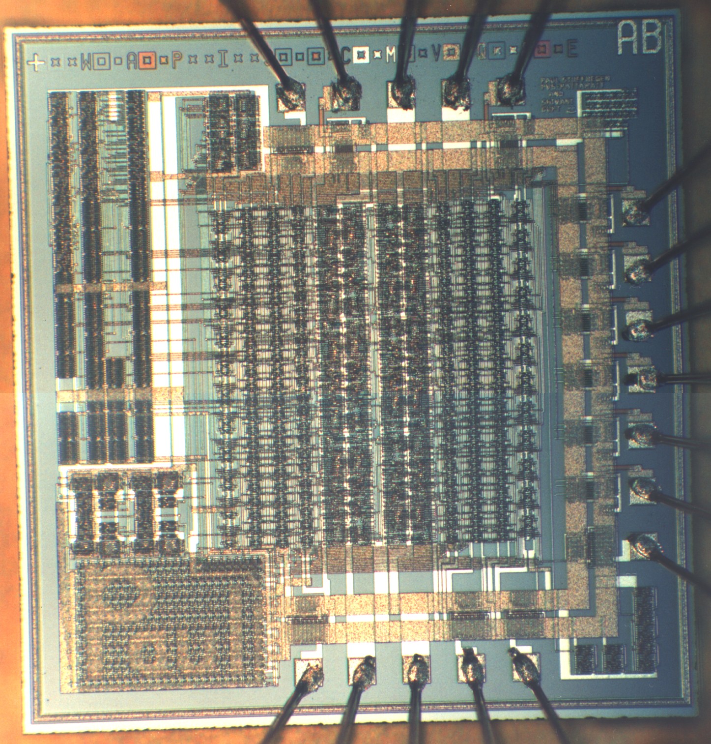
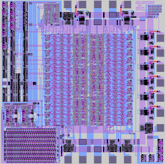
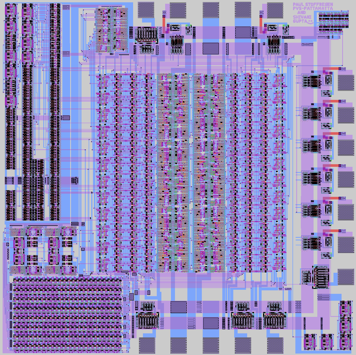
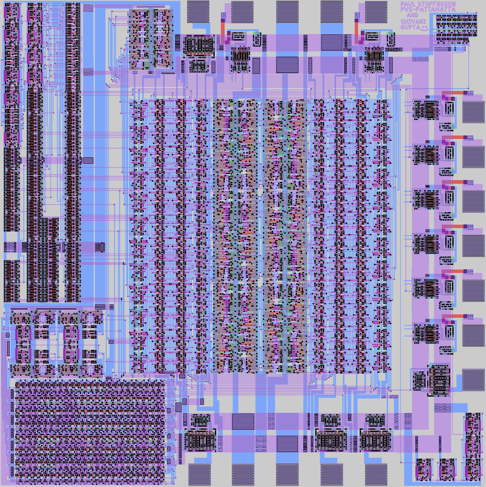
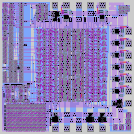 This IC, commonly refered to as "The Decimator", implements a fourth
order (sinc4) digital low-pass filter. The intended application
for this filter is to process output data from a multi-bit sigma-delta
modulator, thus completing a high-resolution A/D converter system.
This IC, commonly refered to as "The Decimator", implements a fourth
order (sinc4) digital low-pass filter. The intended application
for this filter is to process output data from a multi-bit sigma-delta
modulator, thus completing a high-resolution A/D converter system.
The entire design was completed in approximately 10 weeks in the Fall of 1993 by me (Paul Stoffregen), Shivani Gupta, and Srinivas Pattamatta as the project associated with the OSU-ECE graduate VLSI design course (ECE 517) instructed by Richard Schreier.
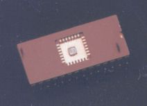
This full-custom CMOS layout was drawn using the CMOSN lambda-based design rules. The layout preview shown here is also available in medium, large, and huge sizes. After the course, the chip was fabricated by MOSIS using Orbit's 2um P-well process on a tiny-chip (2.2mm by 2.2mm) die.
 All four chips fabricated by
MOSIS
were tested (at only moderate speed)
using a microcontroller to feed data into the chip and collect the
output. All four chips produced correct output results!
All four chips fabricated by
MOSIS
were tested (at only moderate speed)
using a microcontroller to feed data into the chip and collect the
output. All four chips produced correct output results!