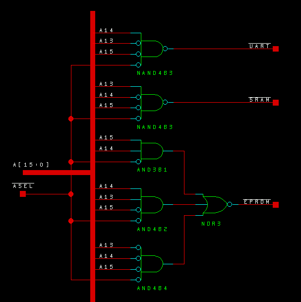
This little circuit provides some simple address decoding,
which would normally be implemented by a logic circuit on
the circuit board. Because this design was implemented in
a Xilinx FPGA chip, adding a bit of extra logic was easier
than putting another chip on the board. The test board
has three chips, a Flash ROM (which also contains the FPGA
configuration bits), SRAM, and a UART.
OSU8: Simple 8-Bit Microprocessor Design; Paul Stoffregen
http://www.pjrc.com/tech/osu8/sch/addr_sec.html
Last updated: November 28, 2003
Status: These pages are a work-in-progress
Comments, Suggestions:
<paul@pjrc.com>Return to OSU8 Top-Level Chip